

Discover how Thomas Edison’s forgotten discovery sparked the creation of the vacuum diode, triode, and ultimately the transistor, the foundation of all modern electronics and the computer age. In this article, we explore the evolution of diodes, semiconductors, LEDs, rectifiers, and the atomic science behind PN junctions, showing how a simple effect inside a light bulb transformed into a multi-trillion-dollar industry.
Scroll to the bottom to watch the YouTube tutorial
Out of the 1,093 US patents held by Thomas Edison, one of them paved the way for modern electronics and the birth of the computer age — a multi-trillion-dollar industry today. But Edison never realised its importance, and he never earned a cent from it.
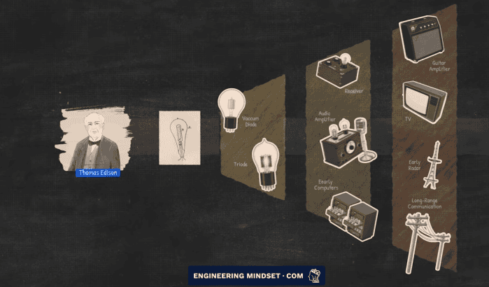
Edison did not invent the lightbulb, but he was the first to make one that was practical and affordable for homes and businesses. And in doing so, he stumbled upon a strange effect that would one day change the world.
He powered the bulbs using DC, or direct current, but he soon noticed something unusual: the glass surface inside the bulb became stained, and always on the same side, the positive side. Curious, Edison and his assistant added a small metal plate inside the bulb and connected it to the circuit. Something remarkable happened. A current was able to flow through the wire. It somehow jumped the gap from the hot filament to the plate. But when they reversed the supply, nothing happened.
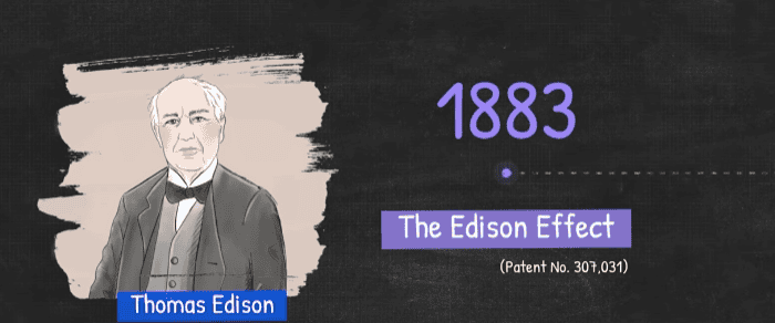
They had no explanation. Still, Edison thought it might be useful and so, in 1883, he patented the effect as “The Edison Effect”. But how it worked remained a mystery, until Fourteen years later, when Joseph Thomson discovered the electron while experimenting with the cathode ray tube . Suddenly the mystery began to make sense. The filament glowed because it was around 1,500 degrees Celsius (2,700*F). At that temperature, it gave off heat, light, and tiny negatively charged particles, electrons. In the vacuum of the bulb, these electrons could move freely. Many were attracted to the positive side, but most missed and collided with the glass, leaving behind that brown stain.
Because like charges repel and opposites attract, when Edison added the metal plate, if it was made positive, electrons leapt across the gap and formed a current. But if the plate was made negative, they were repelled and no current flowed. Edison had unknowingly discovered the first one-way flow of electrons in a vacuum, the foundation of the vacuum diode. But what could you possibly use this for? It seemed almost useless… until another man realised it could change the world.
That man was John Fleming. In 1904, Fleming was trying to solve a problem with early radio communications. At the time, transmitters were basic and used sparks to send bursts of radio waves. Which is only useful for morse code.
Receivers relied on devices called coherers, tubes filled with iron filings. Normally, the loose filings had high resistance, but when a burst of radio waves struck them, they clumped together, lowering the resistance so current could flow. The problem was they had to be reset after every pulse, making them slow and unreliable.
Fleming hated it, he needed something better. Then he remembered the mysterious Edison Effect, could it be the answer? He built his own version of Edison’s bulb and connected it to his radio circuit. Incredibly, it worked. Fleming had created the world’s first practical and reliable vacuum diode.

Because it only conducted in one direction, it could block part of the alternating current radio wave and convert it into a pulsating direct current signal. Suddenly, radio waves could be turned into audible clicks in headphones. Operators could now hear Morse code clearly and reliably. Yet the radio was still trapped to just morse code, voice and music transmission needed something more.
However, an inventor called Lee de Forest added a simple twisted grid between the hot filament and the plate. By charging this grid positively or negatively, he could control how many electrons crossed the gap. This meant not only could you switch the flow on and off, you could amplify it.
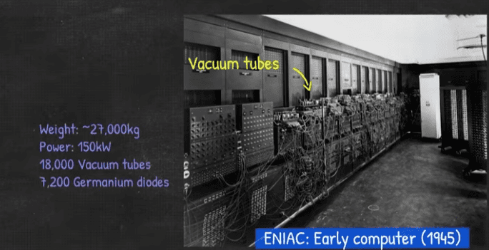
This was the birth of the triode, the first electronic amplifier, and it changed the world. Over the following decades, it made commercial voice transmission and signal amplification possible, and was eventually adapted into logic circuits that powered the first electronic computers. These vacuum-tube computers were enormous and consumed vast amounts of power, but they marked the beginning of modern computing. The triode was also a crucial step toward the invention of the transistor.
While the triode was great at amplifying signals, around the same time, scientists discovered something strange with crystals, they could allow current to flow in one direction but if the polarity was reversed, the current was blocked. This made them ideal for rectifying radio signals, offering a compact, low power alternative to the vacuum diode.

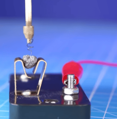
In 1906, Greenleaf Pickard patented a crystal detector for radio. His device worked by pressing a fine wire against a crystal until he found a spot where current could pass in one direction, but not the other. It was crude and unreliable, but it offered the first glimpse of semiconductor behaviour, long before its full potential was understood.
For decades, radios relied on the simple crystal detector, but there was growing demand for something better, something more refined and stable. As our knowledge of material improved, scientists found the answer in Germanium.

One of the first recognizable diodes was the glass-encapsulated germanium diode. Inside it is a tiny piece of germanium doped with antimony to create what we call an N-type region, and a very fine wire making contact to form a P-type region.
N-type simply means this material has an excess of electrons, which are negatively charged. P-type means it has an excess of holes where electrons could sit, and so it behaves as though it’s positive.
At the junction between these two, a barrier forms. When a voltage is applied In one direction, electrons can cross the barrier and current flows. If voltage is applied In the other direction, the barrier expands and current is blocked. This is basically how all diodes work..
However, If we take apart a modern diode, we find silicon instead of germanium, it’s chosen because it can handle higher temperatures and voltages more reliably. But it still has a PN junction. The silicon is usually doped with tiny amounts of phosphorus to make the N-type side, and boron to make the P-type side. Together they form a junction that blocks current in one direction but not the other.
We will look at the atomic structure of how this works later in the article. But first, what do you think this stripe on the case means?
There’s also some numbers and letters which identify the type of diode and allows us to search for the datasheet, which tells us the voltage and current ratings.
The symbol of a diode also has a stripe with an arrow pointing towards it. It’s telling us which way the diode will allow current to flow so we can identify it. But, the arrow points in the direction of conventional current, from positive to negative. Side note. Electrons actually flow in the opposite direction, but its a long story, so to find out why, check this article later.
You can think of a diode like a non-return valve, allowing water to flow in only one direction.
So, if we connect a diode to a lamp in forward bias, with the positive on the anode and the negative on the cathode, when the switch is closed, current flows and the lamp illuminates. Now, if we reverse the diode, when the switch closes, the current is blocked.
So, why does that matter?
Well, that’s useful for protecting circuits if a power supply is connected the wrong way around.
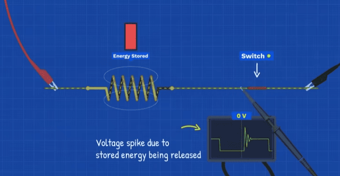
And we also use it to protect circuits from inductors discharging their stored energy when turned off, creating surges. This can be very damaging to electronic components. We can minimize the surges by providing a path to dissipate its energy.
Have you ever noticed your home’s electrical sockets provide AC or alternating current, yet all your electronic devices use direct current? How do you convert AC into DC?
AC has a positive and negative half, the current flows forwards and then backwards repeatedly in the wire. We can insert a diode and block the negative half, creating a pulsating DC supply. But, those large gaps make it impractical to use.
The solution, use 4 diodes arranged in a bridge rectifier design.
The positive half can only flow in this direction, the negative half can only flow in this direction allowing us to fill in the gap. It is still pulsating, but we can add a capacitor to smooth this out and power our devices.
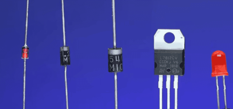
But, the diode can do so much more, and we’re going to discover the main types.
When current flows through a diode, there’s always a small voltage drop, about 0.7 volts in a silicon diode. That energy is lost as heat, and we can calculate the energy lost. By using a thermal imaging camera we can see the diode warms up.
But, if we remove the resin case of a diode, then remove the infrared filter from a camera, we can see it emits infrared light from the semiconductor layer. But, the human eye can’t see infrared. What if we could push that light into the visible spectrum.
That question gave birth to the LED, light emitting diode. We will understand how these work in just a moment. But, these devices were so efficient at producing light in comparison to all other existing technologies, they quickly replaced them.
Although one of these colours was very difficult to produce, comment below if you know which one and why.
Of course, standard diodes have limits. Push them too hard in reverse bias and they’ll break down. To prevent destruction, engineers created the zener diode.
A zener diode is designed to break down at a precise voltage without being damaged.
For example, an ideal 5.1 volt zener will block current like an open switch until the applied voltage reaches about 5.1 volts, then it begins to conduct, and the circuit current increases. Notice the zener voltage remains nearly constant so the voltage across the resistor will have to increase as the supply voltage increases.
Another useful variation is the Schottky diode. Instead of a PN junction, it uses a metal–semiconductor junction. This gives it a much lower voltage drop, typically 0.2 to 0.4 volts instead of 0.7. That means less wasted heat and much faster switching, which is vital in high-frequency circuits. The trade-off is they can’t handle as much voltage, and they tend to leak more current.
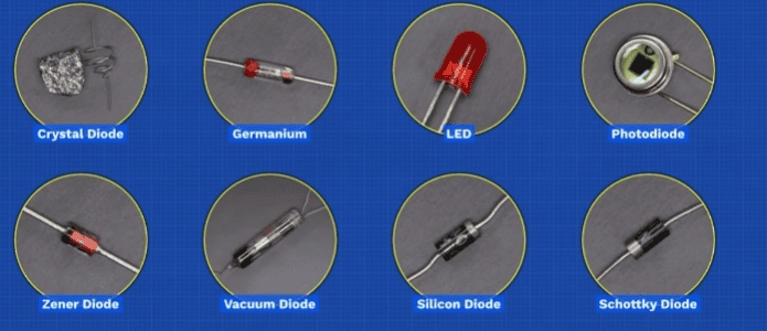
These are just a handful of diode type, there’s even stranger ones we haven’t got time to discuss here, but you can leave me a comment and tell me which type I should cover next.
To really understand why all this works and how leds produce visible light, we need to zoom right down to the atomic level. All materials are made from atoms. Atoms are so small that this cubic centimeter of copper contains over 84 sextillion atoms. An atom is just a collection of 3 particles, the electron, proton and neutron. Different elements have different numbers of these particles.
At the centre of every atom is the nucleus, which contains the protons and neutrons. Around it are orbital shells where electrons sit. Each shell can hold only a certain number of electrons, and an electron must have the right amount of energy to be accepted into a given shell. The further a shell is from the nucleus, the higher the energy required. The outermost shell is called the valence shell. When atoms bond together in a solid, these valence shells overlap each other merging into a valence band. Above it we have the conduction band where electrons can move freely.
In conductors like copper, the conduction band is very close to the valence band, so electrons can reach this and move freely around the material, allowing current to flow easily through them. which is why we use copper wires to distribute electricity.
And to protect us from that, we use insulators like rubber, because the conduction band is much further away, so electrons can’t reach this and remain tightly bound to their atom. But semiconductors like silicon sit somewhere between these. The conduction band is close enough that electrons can reach it, but only if given a little extra energy, from heat, light, or a small voltage.
In a diode, the N-type and P-type regions have different energy band levels. When forward biased, an electron gains enough energy to cross the barrier and moves from the conduction band of the N-type side to the valence band of the P-type side.
By dropping to a lower energy band, it releases a small amount of energy in the process.
That energy is released as a photon. In silicon, the photon has a wavelength in the infrared region, so we can’t see it. But scientists mixed other elements to form new semiconductors which produced larger bandgaps and different wavelengths.+
That pushed the photon energy into the visible spectrum. This is how the light-emitting diode, or LED, was born. Different band gaps give us different wavelengths and we see these as different colours.
And just as light can be emitted from diodes, it can also be absorbed. This is a photodiode. A photodiode works in reverse, producing current when photons hit it. This makes them useful as light sensors and this is essentially the same principle behind how solar panels work. But how do you even produce a PN junction to make this possible?
The real leap forward came when scientists at Bell Labs learned how to purify silicon. They could then melt the pure silicon in a crucible, and by dipping a seed crystal into the melt and slowly removing it, other silicon atoms would attach to this and continue the orientation, producing a single crystal ingot.
During this process, they could introduce tiny amounts of boron or phosphorus to form precise P-type and N-type regions. With this breakthrough, diodes could be manufactured reliably and consistently, and the age of semiconductor electronics began.
But designing electronics is still difficult. Just like a diode, there is a barrier, except this barrier isn’t made of silicon, it’s made of math, physics and the fear of not understanding.
Luckily, our sponsor Brilliant makes learning easy with their fun, hands-on interactive lessons.
Their new digital circuits course lets you see the concepts you’re learning, making it fun so the ideas actually stick. If you want to brush up on circuit basics, they have that covered too. The visuals and interactive problem solving helps you build understanding from the ground up.
And with the Brilliant app, you can learn anywhere. Making it easy to build critical thinking skills through problem solving and not memorising.
Because with Brilliant you learn by doing, they have thousands of interactive lessons across math, science, programming, data analysis, and AI, all the skills you need to become a brilliant engineer.
To learn for free on Brilliant, 👉 click HERE, or you can scan the QR code onscreen on the video.
Brilliant’s also giving our viewers 20% off an annual Premium subscription, which gives you unlimited daily access to everything on Brilliant.


")


")

")


