Scroll to the bottom to watch the YouTube tutorial.
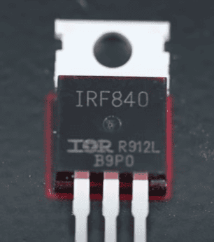
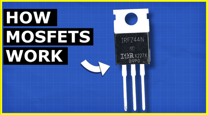
This is a MOSFET! Inside, there’s just a tiny piece of semiconductor. But these components are so important, we find them everywhere.
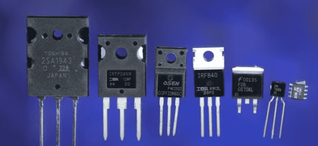
Mosfets look something like this. They come in many shapes and many sizes. They are represented with symbols like these in engineering drawings. I’ll explain those later in the article.
Mosfets have 3 pin terminals, and we call them the gate, drain and source. Sometimes the terminals are in a different order, but, we can check that on the manufacturers datasheet. You can find that online using the part number printed on the front of the component.
I want you to imagine water flowing through a pipe, we can block the flow with a disc. There is a hole in one side of the disc, so if we slide the disc across, we can let water flow again. The disc is spring loaded, so it is normally closed. Another pipe connects to this disc and the pipe is filled with water. If a small pressure is applied to this pipe, it won’t be enough to move the heavy disc, but, at a certain pressure, the disc will begin to move to allow the water to flow, as we increase the pressure, the disc fully slides across and the water can fully flow. But if we remove the pressure, the gate closes and the flow of water stops. This is basically how the mosfet works.
If we take a lamp and we connect it to a power supply, it will turn on. If we insert a switch, we can manually control this. If we insert a mosfet between the drain and source pins, the lamp will remain off, until we apply a voltage to the gate pin. And that means we can use a controller or sensor to turn the lamp on automatically.
But, if we vary the voltage on the gate pin, we can vary the current flowing through the main circuit. That means we can also dim the lamp, as well as turn it on and off automatically.
Instead of a lamp, we can control a relay and the relay can control an AC circuit, and that means we can turn an appliance on and off automatically, and even remotely.
We could also control the speed of a DC motor. The motor can rotate forwards or backwards, depending on how we connect the power supply. But, using mosfets, we can automate and change the direction.
Some electrical loads have a high current, which causes the mosfet to heat up, so we attach a heatsink which increases the surface area with the air and helps cool it down.
For example, this DC power supply, uses mosfets. The mosfets are attached to very large heat sinks. Without them, they quickly rise in temperature.
We can turn mosfets on and off extremely fast by using a pulse width modulating signal. That lets us efficiently control the brightness of an LED light.
We have an entire tutorial on how to design and build that circuit, check it out HERE.
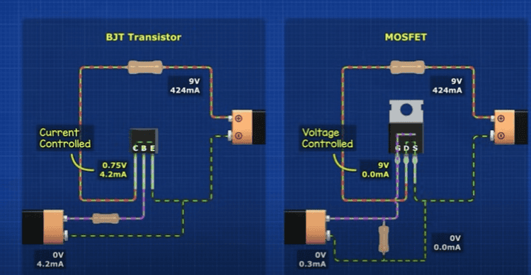
OK but why can’t we just use a transistor? Well a BJT transistor requires current to be applied to the base pin and that wastes energy. A mosfet only needs voltage, almost no current flows, so the circuit is more efficient and easier to design. MOSFETS can also handle much more current.
These larger versions are through hole type, we use them on test boards but also PCB’s. These smaller versions are surface mount type, and we use these in compact electronics. These multi-pin versions are just multiple mosfets combined together but typically there is just one mosfet per device.
Try and build this circuit yourself.
Take a 9 volt battery, connect it to one side of a lamp, connect the other side to the drain pin of a mosfet, then connect the source to ground. Take another wire and connect this to the gate pin. Your circuit should look like this. Notice the lamp is off. But, if we connect the gate wire to the 9 volt supply, it will activate the mosfet and the lamp turns on. Current is flowing through the circuit like this.
Now, If we disconnect the voltage to the gate pin, the lamp remains on. And that’s because the mosfet is now stuck. The gate terminal acts like a capacitor and stores charge. If this charge has nowhere to go, the mosfet remains activated. We can discharge the terminal by providing an exit to ground, which will deactivate the mosfet.
When the mosfet is fully on, no current flows on the gate terminal. But, when the mosfet is changing from off to on, electrons rush into this terminal for a split second, so there is a large in-rush current flowing.
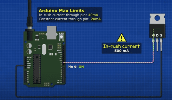
If you are using something like an Arduino to power the mosfet, the current passing through, could damage or destroy the board. So we need to add a resistor to the gate pin to limit the current.
To discharge the mosfet, we need a path to ground. Now we can’t use just a wire, because too much current will flow. So we place a high value resistor here. When the Arduino energises the gate pin, a small current will flow through the resistor but the mosfet gate pin receives the full voltage. When the pin is de-energised, the stored electrons can escape down to ground.
If we place the resistor on the right side, we would create a voltage divider, so less voltage is provided to the mosfet gate pin. For this reason, the left side is often preferred.
For the next circuit, we again connect the 9 volt battery to the lamp and the lamp to the drain terminal. Then connect the source to ground. Then we connect the battery to a resistor and then to a potentiometer. We connect the end of the potentiometer to ground and we connect the centre terminal to the gate pin. The circuit should look like something like this.
The mosfet will be activated so the lamp turns on, the resistance is so high here that almost no current flows through the resistor, we just get a voltage. When we disconnect the power to the resistor, the mosfet drains through the potentiometer.
If we apply the voltage again, we can rotate the potentiometer to increase the resistance and that reduces the voltage available at the gate. As the gate voltage reduces, the mosfet begins to deactivate, increasing the resistance between the drain and source, so the lamp becomes dimmer and dimmer until the mosfet completely deactivates and the current is blocked.
So we can turn a circuit on and off, or we can vary the gate voltage to vary the resistance.
We also have a full tutorial on potentiometers, you can check it out HERE.

You can also buy our merch! This really helps to support the channel. Check it out HERE.
We have two main types of mosfet. The enhancement and depletion type. Enhancement is normally off, depletion is normally on. Applying a gate voltage activates or deactivate the mosfet.
We can think of enhancement type, like water in a pipe blocked by a disc, the water pressure on the gate forces the disc to move and this will allow the water to flow.
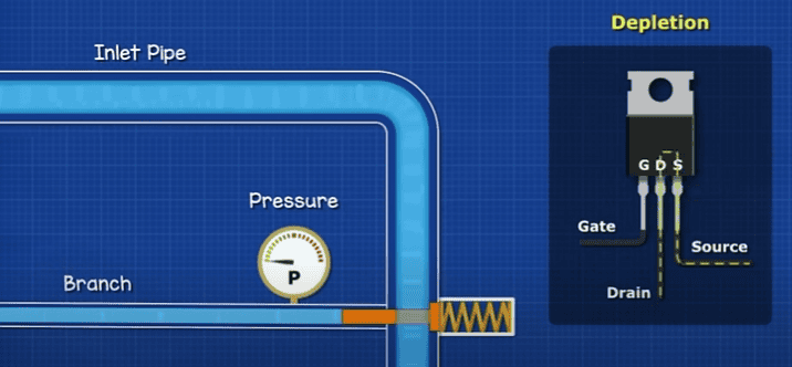
And we can think of depletion type, like water being able to flow through a hole in the disc, but water pressure on the gate forces the disc across which then blocks the flow of water.
These components will look almost identical. but, looking at the symbols, we can see the enhancement type has a broken line across the terminal, indicating it is normally off. However the depletion type has a straight line, indicating it is normally on.
Both of these mosfets come in either N channel or P channel versions. If we look closely we can see there is a small arrow indicating this. This arrow just refers to how the semiconductor is manipulated, but I’ll explain that in just a moment.
For the N-channel, we apply a voltage across the drain and source terminals,
For enhancement type: a positive gate voltage, with respect to source, decreases drain-source channel resistance, turning it on.
For depletion type: a negative gate voltage, with respect to source, increases the drain-source resistance. Turning it off. I’ll explain negative voltage in just a moment.
For P-channel, we apply a voltage across the source and drain.
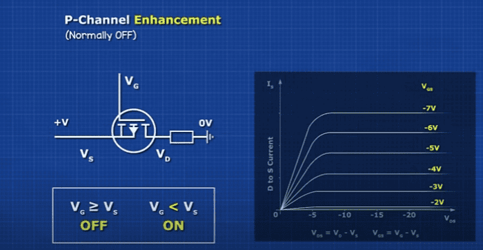
For enhancement type: a negative gate voltage, with respect to source, decreases resistance, turning it on.
For depletion type: a positive gate voltage, with respect to source, increases resistance, turning it off.
Negative voltage sounds confusing, but even a battery can be a negative voltage, it just depends where we take reference from.
In this case if we had 9 volts on the gate but 0 volts on the source, then we have a positive 9 volts so the mosfet is off.
If we had 9 volt on the gate and 9 volt on the source, we would have 0 volts of difference.
If we had 6 volts on the gate and 9 volts on the source, then we have negative 3 volts, so the mosfet is on, but not very much.
Although If we had just 1 volt on the gate and 9 volts on the source, then we would have negative 8 volts. so the mosfet is fully on.
Inside a mosfet, we just have a tiny piece of semiconductor material.
The drain terminal connects to a copper plate, the semiconductor is attached to this and we have some small wires connecting the source and gate to their respective parts.
The semiconductor will probably be made of silicon, which looks something like this. We also use this in LED’s, diodes and solar cells.
Inside, we find silicon atoms. The silicon atom has 14 electrons, with 4 in its outermost shell, known as the valence shell. Silicon atoms are most stable when they have 8 electrons in their valence shell, but they only have 4.
So, they will share an electron with each of their neighbours to achieve this. We call this, covalent bonding.
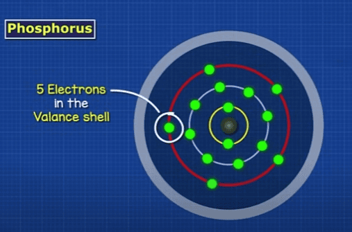
We can take another material, like phosphorus, which has 5 electrons in its valence shell, and add this into the silicon. We call this doping. Four of the phosphorus electrons will be shared with a neighbouring atom, and this will leave 1 electron spare. This electron is free to move around the material. Electrons are negatively charged, so we call this N-type doping, because this material now has an overall negative charge.
We take another material, such as Boron, which has only 3 electrons in its valence shell, and mix it with some silicon. The boron won’t be able to share an electron with each of its neighbours, so a hole has been created where an electron can occupy. As electrons are negatively charged, the holes are considered positively charged. So this is a P-type material.
This gives us N-type and P-type materials. Whenever these materials are joined, we have a PN Junction. At this junction we get a depletion region. Some of the holes move across and some of the electrons also move across. But, this will form a barrier, with a slightly positively charged region and a slightly negatively charged region. This creates an electric field, which prevents more electrons or holes from moving across.
For the N-channel enhancement type, We find a substrate, or base layer, made from P-type silicon. Attached to this are two small segments of heavily doped N-type material. Notice we have joined two materials here, so we have a PN junction which causes a depletion region.
The drain terminal connects to one of the N-type segments, the source terminal connects to the other. The metal body usually connects to the underside of the substrate and this is typically connected to the source pin.
That is why the symbol shows a drain terminal, a source terminal and a base terminal, with the base connected directly to the source.
We then have a layer of silicon dioxide ( SiO2) over the semiconductors, a metal contact pad is placed on top of this, which forms the gate terminal.
The silicon dioxide is an insulator with an extremely large resistance. This keeps the gate pin separated from the semiconductor, and prevents current from being able to flow through this.
It is also a dielectric material. So if we apply a positive charge on one side, a negative charge builds on the opposite side, and an electric field forms between them. Just like a capacitor.
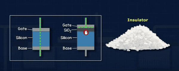
So we have, metal, dioxide, semiconductor, and the voltage on the gate pin creates an electric field which affects the material of the transistor. Hence we have, mosfet.
If we apply a voltage across the mosfet, from drain to source, no current will flow. The depletion region is blocking the path. The more voltage we apply, the wider the depletion region becomes. This is called the cut off region.
You can see from the PN junctions that we basically have two diodes. But because the body is connected to the source, which is grounded, only the right-side diode is activated, which is in reverse bias.
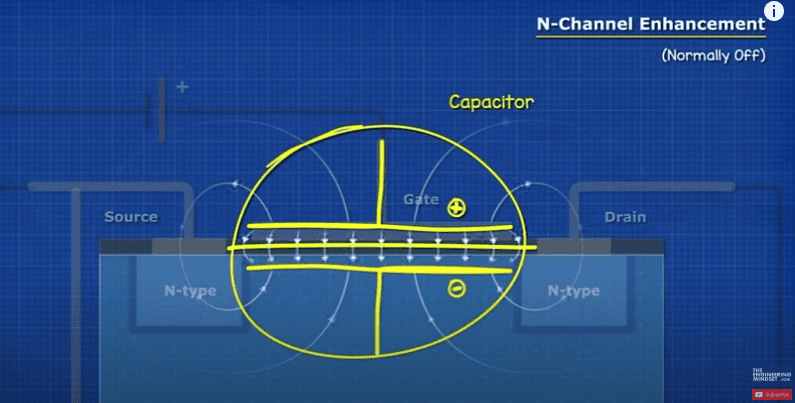
When a positive voltage is applied to the gate pin, an electric field is generated between the metal sheet, through the silicon dioxide and into the semiconductor layer. This region is acting like a capacitor.
Electrons within the P-type layer will be attracted to this and rise up towards the gate terminal, but they can’t pass through. Think of it as something like two opposing magnets being attracted through a barrier.
As the gate voltage increases, the attraction becomes stronger and stronger, more electrons are pulled into this region, some of the holes will be filled and some holes will also be repelled away.
Electrons will then begin to assemble along the surface, creating a channel of negatively charged electrons. This is why it’s called an N-channel mosfet.
This creates a new depletion region, extending between the drain and source terminals, connecting them together. Removing the gate voltage breaks this depletion region and the electrons and holes will return.
If a small voltage is applied, the channel won’t fully form. But, at a certain voltage the channel will form. So, when we apply a voltage across the drain and source, current will begin to flow.
The point at which just enough voltage is applied to the gate, to allow current to flow, is called the threshold voltage. This voltage is different for each mosfet.
As we increase the gate voltage, the channel becomes wider.
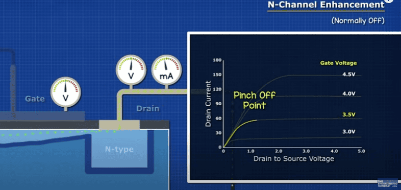
As we increase the drain to source voltage, the resistance decreases and the current increases linearly, we call this the ohmic region. But, the depletion region becomes stronger on the drain side because of the reverse bias diode, this will begin to narrow the channel at one end, we call this the pinch off point. Because of the current flowing through the channel, the channel won’t fully close, but the current can’t increase any further. We call this the point the saturation region. To increase the current we need to increase the gate voltage. You can find all this information in the manufacturers datasheet.
Notice the small arrow on the symbol points towards the layer. This indicates that the carrier, in this case electrons, are being pulled up to form the channel.
The N-channel depletion type, has a very similar design, except that we add a thin n-type layer, forming a physical channel between the source and drain n-type layers.
When a voltage is applied across the drain and source terminals, current flows through the channel.
When a negative voltage is applied to the gate, the electric field generated pushes the electrons out of the channel, and pulls holes into the channel. This will begin to narrow the channel. The more voltage we apply, the narrower the channel becomes. Eventually this will block the flow of current through the mosfet.
So we can use a voltage to turn a circuit off using this mosfet.
However, when a positive voltage is applied to the gate, electrons will be attracted to this, they will begin to collect along the N-type channel which will increase the channel and allow more current to flow.
With the P-channel enhancement, the base layer is made from n type material with heavily doped p type layers, on the source and drain terminals.
When we apply a negative voltage to the gate; the electric field will repel the electrons into the substrate and attract holes along the surface of the insulator. This will begin to form a channel between the two P type layers. The further we increase the voltage, the larger the channel becomes.
Now when we connect a voltage across the source and drain; current will begin to flow through this channel. With the P channel depletion, we have an N type substrate with P type regions at the drain and source. A layer of P type material forms a physical channel between these two terminals. When we apply a voltage across the source and drain, current is able to flow through the channel. When we apply a positive voltage to the gate, this causes a positive charge on the plate which repels the holes out of the P channel and into the substrate. Electrons from the substrate will be attracted up towards the gate terminal which causes the channel to reduce in size. This decreases the current flow between the source and drain terminals. As we increase the gate voltage, the depletion region blocks the flow of current between the two terminals. So we can use this device to turn a circuit off by applying a voltage to the gate terminal. However if we apply a negative voltage to the gate terminal, the holes will be attracted to the negative charge and so the channel increases, allowing more current to flow through the mosfet.

